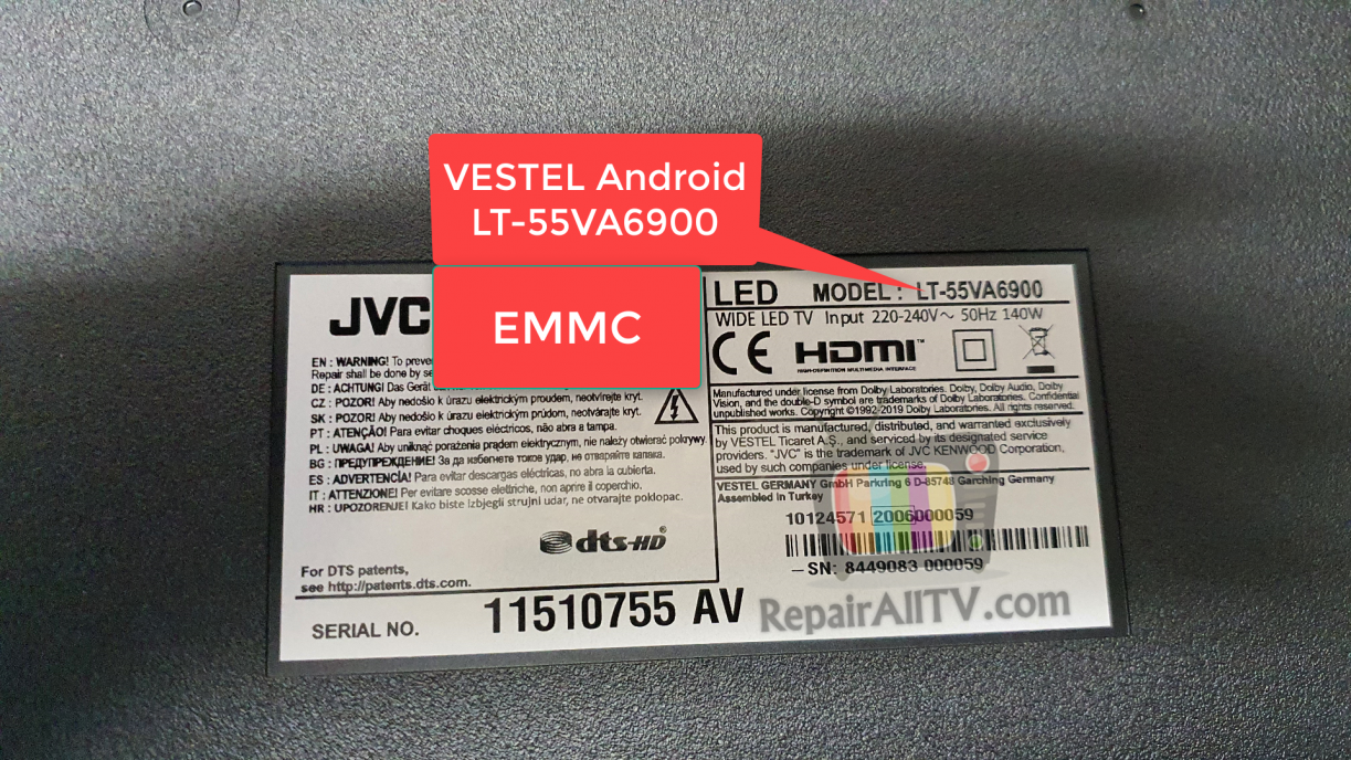
JVC LT-55VA6900 17MB170 vestel Emmc KLM8G1GETFB041
jvc lt-55va6900 17mb170 vestel Emmc klm8g1getfb041 Android Download
jvc lt-55va6900 17mb170 vestel Emmc klm8g1getfb041 Android Download
TV MODEL LT-55VA6900 Android
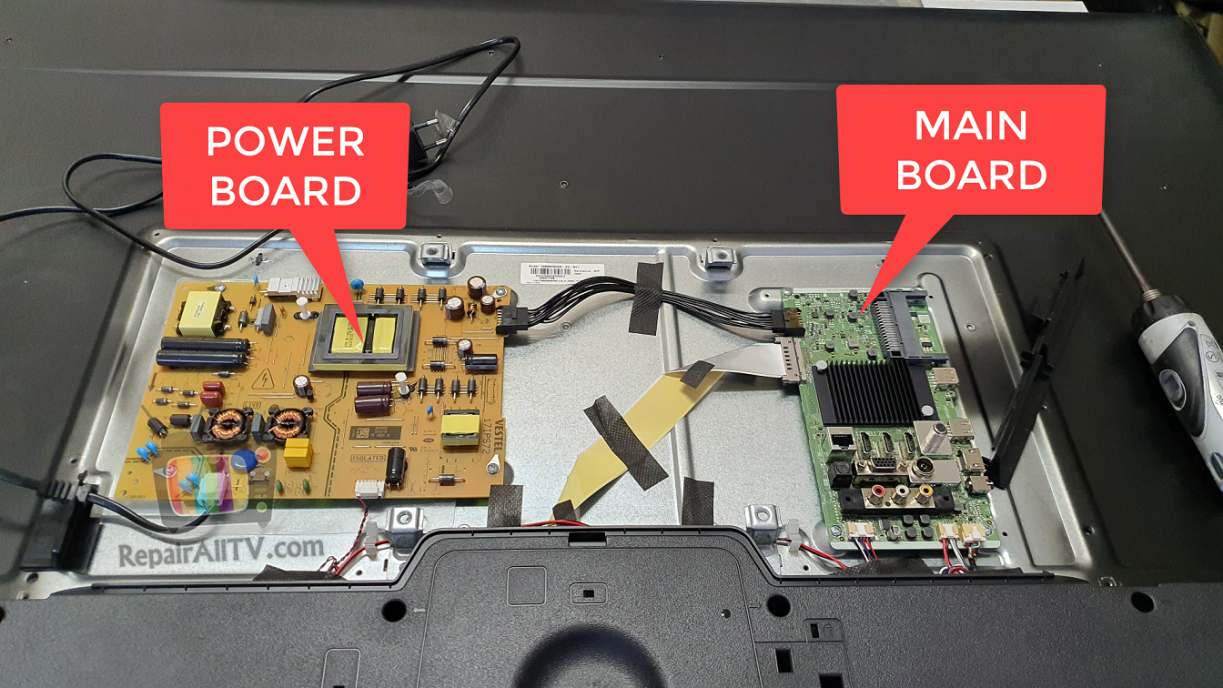
POWER BOARD MAIN BOARD
JVC LT-55VA6900 17MB170 vestel Emmc KLM8G1GETFB041 Android Download
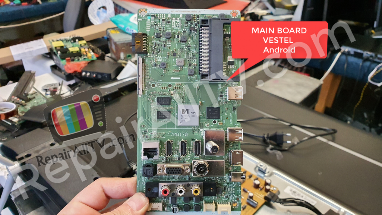
MAIN BOARD VESTEL Android
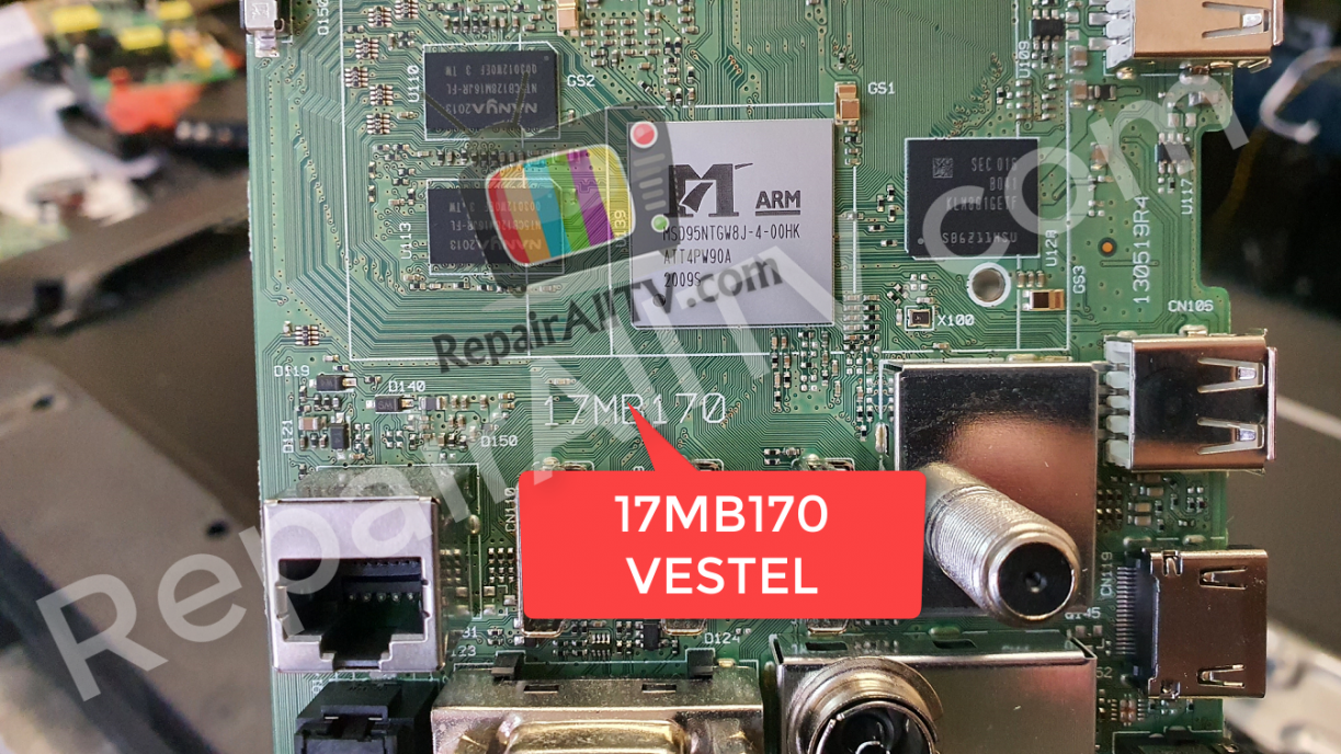
17MB170 VESTEL
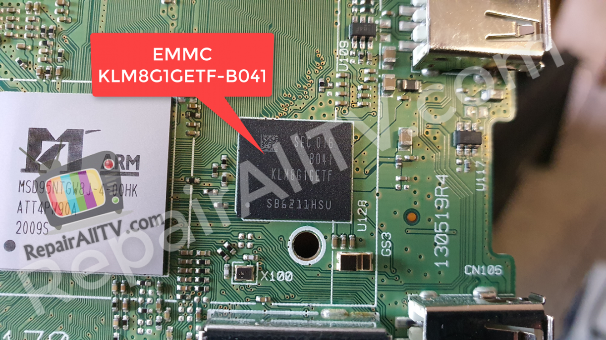
KLM8G1GETF-B041 IMAGE
to see EMMC pinout photo as well as to download EMMC BIN Firmware. you must subscribe
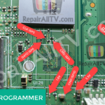
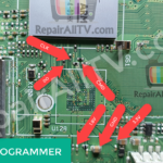
PROGRAMMER TNM5000 ISP INFO
Programmer ISP Cable EMMC pin
ISP PIN 1 CMD
ISP PIN 3 RST-n(Reset) (mandatory)
ISP PIN 5 CLK (Clock)
ISP PIN 6 DAT0
ISP PIN 8, 10 VSS (GND)
Vcc of Chip Must be ON. Reset is needed only when circuit reset is not working.
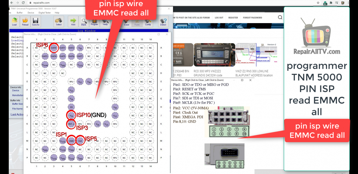
Note 1: After Selecting EMMC, programmer will be switched to Report view.
because EMMC files are too large and can’t be viewed by hex editor.
you can switch back to hex editor by unmarking the report button.
Note 2: Load & Save buttons has no use in EMMC nand. you must select filename
after pressing read or program buttons. File will be saved automatically with
Boot1, Boot2, RPMB, EXT_CSD extensions for different parts of the chip.
Note 3: After pressing read or Program, EMMC size and type will automatically
be Detected.
Note 4: Use Config Window for selecting Different Parts of the chip for read and write.
Also, chip Size and name is read from the chip and can be viewed in this window.
Note 5: Erase is for total chip erase. before Programming Each part, Programmer
will erase it automatically, so no need for chip erase before program.
Note 6: Only First 192 byte of EXT_CSD is writable by users and Some of these bytes
are read-only and some parts are one-time programable so if you write over these areas,
you get Write error.
Note 7: in most cases, Reset Pin is not necessory, Power on/off the device for reset
to see EMMC pinout photo as well as to download EMMC BIN Firmware. you must subscribe
RT809H PROGRAMMER ISP INFO
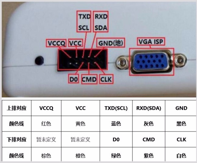
RT809H PROGRAMMER ISP INFO
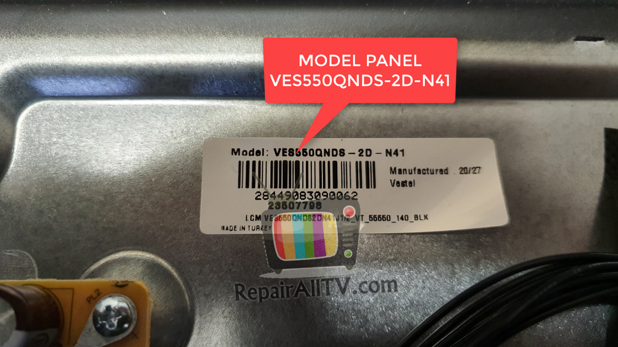
model panel VES550QNDS-2D-N41